Saturday 29 August 2015

My Method for high speed PCB design

High Speed Design - Project

Step by step implementation of high speed design constraint

  • Some design rule creation in schematic capture itself.
  • Net list transfer to PADS layout.
  • Identify High speed design Nets.
  • Creation of
    • Net classes
    • Matched Net Length objects
    • Differential Pairs
    • Conditional Rules
    • Pin - Pairs (if required)
  • Using design guides as a reference create a Line Sim document for critical NETS and run pre-layout Signal Integrity simulation with appropriate models for drivers and receivers.
  • Based on simulation result determine optimum termination & maximum NET length as well as no. of vias to be used. (For critical Nets like Clocks I use a maximum of 4 vias).
  • Component placement keeping simulation results in mind.
  • After complete component placement run pre-layout SI analysis using "Manhattan Length".
  • Start the routing process in PADS Router.
  • Fan-out high speed signals from outer layers to proper strip line layers.
  • Route all high speed Nets with proper design constraint based on design rules or simulation results.  
  • Layer Stack-up creation
    • No. of Signal Layers                                       ---   Based on total no. of Nets
    • No. of Plane Layers                                        ---   For distribution of GND and PWR Nets
    • Spacing between Plane & Signal Layers        ---   Depends on Cross-talk tolerance
    • Spacing between Plane Layers                       ---    Based on inter-plane capacitance
    • Track width in Signal Layers                          ---    Based on trace impedance
    • Gap between Signal Layers                             ---   To obtain specific PCB thickness
  • Once high speed critical nets are routed power supply routing can begin based on sample layout on data sheets.
  • Fan out GND connections for power supply nets. If required separate analog and digital ground.
  • Determine proper decoupling @ all voltage rails specially the ones driving single ended wide buses.
  • Run Power Integrity simulation for
    • dc drop
    • impedance vs frequency curve
    • simultaneous switching noise
  • Route non-critical nets and complete the first iteration of layout.
  • Post layout SI, PI and Thermal simulations.

Tuesday 18 February 2014

Sensor Characterization Bench

Currently I am working on an interesting project that I would like to share. It is the design of complete instrumentation and electronics for a sensor characterization chamber. Let me first explain what a sensor characterization chamber is. In our Sensor hub many MEMS engineer design various types of low power low cost sensors to be implemented on the field. In order to plot the proper characteristics of these sensor one needs a characterization chamber. It can also be used to calibrate the response of a sensor to a much higher standard coming from ultra precise standardized sensor. It also helps to plot how the sensor behaves by simulating various environment like high humidity, high temperature presence of other gas which mixes with the targeted gas and contaminates the data. Let me share a block diagram of the various instruments used for the characterization chamber.
 Most of the block diagram is self explanatory. The main controller controls the environment inside the chamber. User can use per-programed settings or even can use custom settings while using the chamber with their sensors. The fan controller is used for expelling the gases once the process is finished and the pump controller is used to increase or decrease the internal chamber pressure. The gas input controller lets the user to control the flow and amount of gas into the chamber. For collecting data from the sensor a low noise proper analog interface is used. Which then converts the analog value into a high resolution 16bit digital count. There is provision for storing the data or displaying it to a computer which gives various other functionality. The biasing power requirement for MEMS sensor can be difficult different designs require different voltage some needs constant current whereas some needs both. So a software controlled voltage and current source is dedicated for this purpose. The power module provides appropriate power to different sections.
From designing point of view I have broken the system into 5 independent PCBs. 
  1. Power Module board.
  2. Main chamber controller board
  3. Sensor power, Sensor interface, DAC and PC interface all in one board.
  4. Gas input controller.
  5. Fan and vacuum pump controller.
As I go about designing each board I will post updates as necessary.
I will start with the Fan and vacuum pump controller.

Friday 21 June 2013

DC Power adapter Noise

In my last blog we talked about how noise can creep into and destroy your seemingly clean system when you have a switching device in the vicinity. I thought as we were already discussing the topic of noise let me also give you another example of a noisy source. 

Now a days every one is familiar with dc power adapter which comes with various electronic equipment including mobile phone chargers, microcontroller development board and other stuff. Pretty handy little device light weight directly plug into wall socket and provides +12V, +5V, +9V voltage (depending on the rating) to power or charge your device.

What is inside these devices are called switching regulator circuitry rather than linear regulator. Most advantage of switching regulator is the power dissipation within its series pass transistor is minimum giving it ultra high efficiency of more than 90% some times. However the circuitry is complex and suffers from noise being injected in the output dc rail. The noise is a result of the high frequency switching which is used internally within the regulator.

In most of the case when you are designing your circuit you will have the output of the adapter to go into a linear regulator say 7805 to get a low noise regulated dc output provided you decouple the output properly. The scheme should look something like this.
 

The output in this case is properly decoupled to reduce noise content in the 5V rail, however the 12V rail remains to be decoupled. I have probed the two Rails with ac coupled channel in my scope to find out the noise content within each of them.

Noise @ +12V Rail ~ 96.8mV
Noise @ +5V Rail ~ 11.2mV
I have excluded the transient peaks since I was again using a breadboard.
Clearly from this the noise at the 12V rail is substantially more. The 5V rail being a linearly regulated one along with proper decoupling shows much lower noise it would be much more cleaner on a PCB. Now most of the times may be you wont use the +12V rail in your circuit. But sometimes say if you do want to include both the rails (for high voltage applications) you definitely want to do something about the noise.


This is the same noise with the scope speed up. The switching frequency of the switching regulator can be clearly seen.
Simple solution is just decouple the +12V rail as well.


With input decoupling capacitor. 

The Noise on the 12V rail is greatly reduced.
This is a simple and effective way of having two power rails within your circuit.

Tuesday 18 June 2013

Noise Analysis for the 555 timer - How to not ruin your design.

Noise Analysis for the 555 timer

With modern day advancement in electronics resulting in low power and high speed designs noise becomes an ever increasing challenge for circuit designer. The concept of noise its effect and analysis is quite complex apart from noise which can come into the system from external sources via different forms of coupling via i/o ports, power rail etc certain electronic components also generate noise on their own. Every data sheet specifies those parameters. So dealing with noise is quite a challenging aspect. However in this blog I am not going to get to complex mathematical analysis of noise but show you a rather simple example of what noise can do to your circuit if proper precaution is not taken. 
Let us start with a simple circuit a 555 timer hocked in astable configuration to generate a 4% on time duty cycle. Before I go any further let me tell you if you have switching elements in your circuitry there is a high chance you have to deal with noise issue as switching elements have very high frequency components which can get coupled to other parts of the circuit. 555 timer is a switching element hence we have to deal with noise. This is the circuit we will be dealing with.
This is a simple circuit used to generate a PWM waveform to blink a LED at the output. It can also provide voltage control to other parts of the circuit. Generally the duty cycle you get from 555 timer in normal astable configuration is always greater than 50%. In order to get around this I used diode D1 which bypasses R2 hence duty cycle can go below 50% now. As usual the circuit works perfectly fine giving duty cycle of 4% @ 2.93Hz. Here is a grab from the oscilloscope.

The rise time for this square wave output is about 130nsec. This is from a cheap Chinese 555 timer IC. The CMOS version of 555 can have very low rise time. Lower the rise time steeper will be the slope and the wave form will contain more high energy stuff and likely to produce more noise. Let us look at the Rise time curve.
Notice the measurement window at bottom left the rise time is shown there. With 130nsec still this chip will inject considerable noise.
Look at the circuit diagram notice the power pin for the IC (pin 8) it lacks a decoupling capacitor. The only decoupling the +5V rail gets is from the decoupling capacitor at the voltage regulator output. As the V_reg was quite far away pin 8 requires its own decoupling cap.
Now let us look at the power rail with our channel 2. Channel 2 is ac coupled so we are only looking at the noise which sits over the +5V dc.
Ok before you panic let me tell you this that I have built the circuit on a bread board not the ideal case when you want to do noise analysis. In a printed circuit board this effect would be somewhat reduced but always be there to ruin your design unless you do something. Ok coming back to the diagram look at the delta y measurement I have done that gives the peak to peak noise its almost half a volt. That much of noise is being injected into the rail. Now if you feed your other parts of circuitry with this rail say your precision low level amplifier your design is done. Most probably if your amplifier does not have good supply rejection it will start to oscillate not a good thing for your design. Another thing I noticed when the output is high the amplitude of the noise is low compared to when the output is low. The following picture will clearly show it when I have speed up the scope.
Now just by pacing a single 1uF cap as a decoupling capacitor the noise reduced almost 1 orders of magnitude. I have tried different cap values 0.1uF, 10uF, 47uF etc 1uF works the best.


Let us look at the decoupled version of the noise.
Again look at the delta y measurement the noise now merely is 58mV peak to peak. Still 58mV is not enough for certain application but then we have to design our circuit on a pcb. However a  ferrite bead series with the power rail will prevent some of those high frequency components from going into the power rail and subsequently into other parts of the circuit. Ferrite beads being basically an inductor provides high impedance to high frequency signals thereby blocking some of them. I didn't have a ferrite bead so I use a 1mH inductor not ideal but the noise did decrease a bit.
Here is the final noise result.
Final peak to peak noise with inductor is about 44.8mV.

So here it is an apparently simple circuit can wreck havoc in your design if you don't know the effect of noise. Although I have just scratched the surface of a vast topic but I hope this will give you enough knowledge to be cautious when dealing with switching components in your circuit. Till next time... 


Saturday 1 June 2013

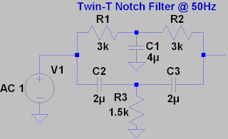
The Twin - T Notch Filter

Before I start let me give an brief I mean really brief introduction of what electrical filters are. Simply electrical filters are filters which filters out unnecessary information i.e. signals from data so that we can get a cleaner low noise output signal. Filters can be used for various applications like selecting frequency multiplexed signals, noise reduction ac decoupling. The last one is going to be the example I discuss here.

Filters can be classified into two categories broadly Passive filters (only R,L,C components) and Active filters (R,C along with active devices like op-amps and transistors). 
For more components, a little more power consumption and a little bit extra cost Active filters yield certain advantages like 
  • Flat passband response.
  • Sharp transition from passband to stopband.
I can go on and on about filters but let me focus on the example. It is really simple and a great example of showing the power of this kind of filter. A very low amplitude signal from a bio-med sensor was to be amplified and sent to the ADC. The input to the amp was in uV range and output from the amp was 2 to 3 volts. In this kind of situation it is best to use a chopper or auto zero amplifier which has low offset voltage however offset voltage is not the problem here.
Before going further let me discuss about the power plane of this board it consist of a single 5V DC BUS which comes from a regulated power supply which is fed from half wave rectified ac signal.
 
During the first attempt I build this circuit by normal layout scheme decoupling the opamp power pins. It was working just fine the ADC readout was ok but sometimes the ADC was producing odd set of values it was completely random. This random value did not fit into the data set points and I was sure this was due to noise being injected either at the i/o pins or the power pins itself. As the noise was considerable I was sure it had to be the power pins. So I probed it and voila... It was the residual 50Hz noise from the AC supply. Although The linear regulator is supposed to produce a clean output still some noise remains and it is being magnified by the op amp output stage.
 
Therefore this is an ideal situation to use a filter at the power pin of the opamp. Now ofcource we can use active band reject filters tuned to reject the 50Hz component from the power line but as most of the power associated in this signal will be in the dc domain with a very narrow band to be rejected active filters will really be a overkill. So are we going to yes a normal passive filter network? The answer is yes and no. The filter network will be passive ok no doubt in that but it wont be your typical LPF or HPF.  Using normal LPF will work but only moderately since they have very soft cut off some of the 50Hz noise will still remain definitely will be of less amplitude but never the less will remain. So we have to use a modification of the normal passive filter. This is where we use the Twin T notch filter.
 
The Twin T notch filter has the similar soft response like other passive circuits suffers from but it has extremely almost like brick wall response at the selected tuned frequency ideal for rejecting a single frequency component like the 50Hz noise. 
How this particular filter works is simply it adds two signals which are 180degree out of phase at the tuned frequency. So the amplitude response at the tuned frequency is extremely low.

However there are certain disadvantages with this filter 
  • The component values have to be precisely matched
  • Very difficult to tune
By applying this filter everything became normal. The random jitter of the ADC readout completely went away. Later I will try to share a screen grab from the oscilloscope showing the noise free signal.

Just wanted to  share this simple yet effective piece of circuitry which you may use in your next project and get noise free result. Till next time...

Wednesday 10 April 2013

FM transmitter unit for Gas Sensor

         I was working in designing a proper low power signal conditioning circuit for a MEMS based gas sensor for quite a while. Now as these sensors are supposed to be deployed in remote isolated areas deep within coal mines it is always advantageous to read the value of these sensors remotely or in a wireless manner. Now RF power transmission within coal mines are highly regulated and operates at strict protocols. The conditions that I was to follow was that my unit should not in no way transmit more than 5W in RF power. So I designed my power amplifier stage around 4W max. 

                Next was choosing the transmission protocol. Now as my system was more or less digital I was initially inclined to go for digital communication scheme. So I choose FSK to transmit serial binary information. Turns out there is a single IC TH72031 from Melexis Microelectronic Integrated system capable of performing the entire FSK operation directly on Digital Data. But further analyzing the scheme although it was very simple presented certain problems. The major being FSK signal with 4W power was not being picked up by the receiver at the supposed distance. Another problem was as FSK IC was generating a variable frequency square wave applying it directly to the antenna produce spurious transmission at frequency bands it is not supposed to transmit. The solution was to use a very costly RF band pass filter or change the transmission scheme. 

             I choose a good old analog transmission scheme Frequency modulation. The idea was the microcontroller reads the gas sensor value performs internal calculation and calibration and then sends the final digital value via I2C BUS to a 16bit DAC. The then received analog value is properly scaled and transmitted.

              Let me share the schematic for this.
  
  The MAX2606 is a FM generator chip. It uses only one inductor L4 to set the nominal frequency around which the modulation will be done. We apply the analog signal from the DAC with proper scaling (can be tweaked during operation) to the TUNE input.

The MAX2606 output is about 50ohm and is applied to the PA stage and subsequently to the antenna. However the antenna choice and design is not yet complete.

I will be updating as the circuit development goes on...  
 

Saturday 15 December 2012

Smart Digital Thermometer REV A Schematic

Here is the link for the REV A schematic. You will notice that some component values are missing this is because I haven't tuned those values yet soon will be doing so.

How ever for now...

http://www.ziddu.com/download/21121547/page1.pdf.html